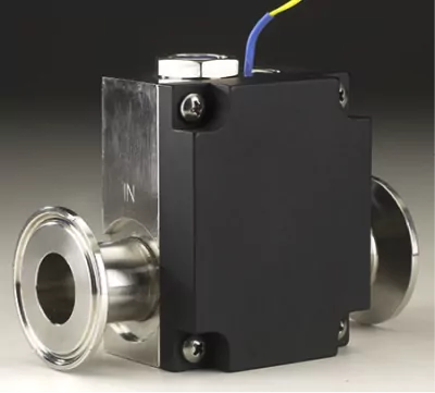
The semiconductor market continues to grow, and it’s not just all those new smartphones. Cars and lighting are the other big drivers, and all this growth means continued investment in semiconductor fabrication facilities and equipment.
Phones, Cars and Lights
Moore’s Law, the observation that the number of transistors on a chip doubles every two years, still underpins technological advances. Chip makers like Intel and Samsung recently introduced so-called “14 nanometer” processes, allowing even more transistors to be packed into a given space. (At 14 nm transistors are some 70 nm apart.) This lets designers add more capabilities, creating phones like the Galaxy S6 and S6 Edge and iPhone S6. Sales of lower-end smartphones are rising rapidly too, with demand from countries like China and India, fueling growth.
Growing numbers of new car buyers are demanding Advanced Driver Assistance Systems like blind spot warning. Coupled with telematics like GM’s OnStar, this has pushed the semiconductor content of the average new vehicle to around $350. As motorists push for more autonomous driving capabilities this number will only grow.
The rise of LED lighting in automobiles and the home is another driver behind semiconductor growth. LED’s are at their heart semiconductor devices, made by manufacturing processes very similar to those for microprocessors. With consumers demanding (or perhaps being pushed into) more efficient lighting, demand for LED’s will likely continue to rise.
The Semiconductor Fabrication Process
Making advanced chips like the Exynos used in Samsung’s Galaxy phones takes over a hundred processing steps. Other semiconductors, while less complex, go through the same basic sequence: A silicon crystal is sliced into wafers. These are lapped, etched, and polished to create a surface ready for the masking and etching steps that create transistors and other devices. Cleanliness is absolutely paramount and these process steps demand great quantities of ultrapure water (UPW) for washing. (The definition of UPW is spelled out in ASTM D5127.)
Protecting Yields and Equipment
Making UPW is itself a complex process, involving putting water through multiple steps. Wherever there are flows there’s a need to ensure the systems are functioning correctly. Leaks and blockages are both potential risks and flow monitoring provides early notification of any problems before they start to affect the process.
The same applies to the actual wafer washing processes. With microscopic filters the risk of partial blockage is ever-present, so a flow monitor provides confidence everything is working correctly. Insufficient flow could mean damaged wafers, hitting yields and proving very expensive.
ChemTec Product Application

This initiates a signal that can be used to trigger an alarm or shutdown the process. Flow monitors like these are a reliable and inexpensive way to protect high value product and equipment. With the semiconductor industry continuing to grow, the indications are there will be many more potential applications for this and similar flow monitors.
Contact us today if you’d like to order a ChemTec product for the semiconductor industry. Our speciality is customization and our engineers are ready to take your call.